Functional simulation of all integrated modules
Let's attempt to do the simulation of the system-wide to load into FPGA.
It creates kite_test.v as the test bench and it summons kite_top module.
The KITE processor begins to execute the program which was written in the memory after reset.
Because it is, it gives only 100MHz CLK and RST continuously from the test bench.
--- kite_test.v ---
`timescale 1 ns of 1ns/
module kite_test ;

reg        CLK, RST ;
wire [3:0] TMDSP, TMDSN ;


initial
begin
  $shm_open ("waves.shm") ;
  $shm_probe ("as") ;
end

initial
begin
  #16000000 ;
  $finish ;
end

initial
begin
  CLK = 0 ;
  while (1)
     CLK = #5 ~CLK ;
end

initial
begin
  RST = 1 ;
  RST = #5  0 ;
  RST = #30 1 ;
end

kite_top kite_top ( .CLK(CLK), .RESET(RST), .TMDSP(TMDSP), .TMDSN(TMDSN) );

endmodule
In the integration simulation, it simulates including the PLL module for a clock generation inside FPGA and the dvi_out module for making DVI signal.
So far, we were using Verilog-XL simulator by CADENCE.
In this integrated simulation, however, we can not use Verilog-XL because it can not carry on mixed language simulation Verilog and VHDL, PLL module is described in VHDL.
We use NCsim by CADENCE instead of Verilog -XL.
NCsim can carry on the mixed language simulation.
To use NCsim, "cds.lib" file is required to set environment.
INCLUDE /opt/XILINX/14.7/ncsim/cds.lib
The simulator specifies all necessary files as follows and executes
them. In the directory which the source of the KITE processor is placed.
And the source of the dviout module is in the dviout directory
Simulation is started by following command;
ncverilog kite_test.v kite_top.v kite.v vram.v memory.v acc.vdec_seq.v
ir.v opcode.v r12.v alu.var.v fr.v pc.v
/opt/XILINX/14.7/ISE_DS/ISE/verilog/src/glbl.v
dviout/DRAM16XN.v
dviout/convert_30to15_fifo.v
dviout/dvi_encoder.v
dviout/dvi_out_native.v
dviout/encode.v
dviout/serdes_n_to_1.v
pll_module.vhd
-V93 +access+r
+nc64bit
-gui
Here, "/opt/XILINX/14.7/ISE_DS/ISE/verilog/src/glbl.v" is necessary primitive in simulation for Xilinx's FPGA.
Check the wave form of the simulation result useing "simvision" is automatic invorked.
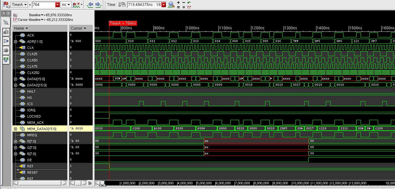
RST is deasserted after PLL becomes stable and LOCKED is asserted.
The program begins to work from here. You can see that a fetched processor instruction is appeared in MEM_DATAO.
The RGB output becomes unknown value from 1100ns. This reason is that unknown values in pipeline register while 2-character period are output before correct values are appeared.
There is no problem in this situation because the DE signal is unasserted. DE signal means charater display timing.
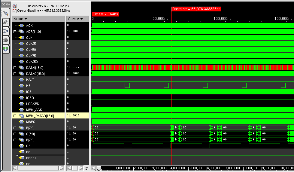
Also, as for the character screen-display, too, it finds that it is working with no problem from the following corrugation.
| Back
|CAD Home
|