The creating of CUI module
We create the CUI module for the KITE-1 microprocessor.
The specification of the CUI module
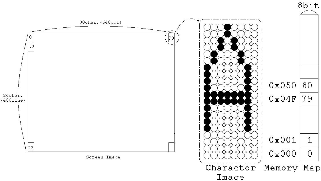
- It displays a character and 80x24 character is on screen.
- One character font is 8-dot x 16-line.
One character has 20-raster, 4-raster is a blank raster. (It isn't displayed).
- Therefore, the dot composition of the whole screen is 640-dot x
480-raster.
Below figures show the screen structure, the character structure and
the memory map for the KITE-1 microprocessor.
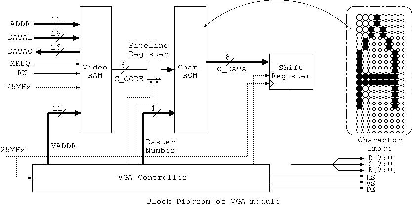
The block diagram of the CUI module
The CUI module consists of the following block mainly.
- Video RAM : The memory which maintains the JIS8 bit code of the character to display in the screen beforehand
Because the total-character-on-screen is 80x24 character, it must be able to store 1920 pieces of Word at 8 bits.
Because it decides using a 8-bit character code this time, 1920 pieces of Word should be able to be stored at 8 bits.
- Charactor ROM : The memory which stores the character information of the character beforehand
Because it is 256 characters in case of the JIS8 bit code, when the composition of 1 character is 8x16line, 8-bit 4096 Word gets to need.
It controls the blank line (it isn't displayed) of the remainder with 4 lines in the following CUI Controller and it should realize a display.
- It shifts the dot data of the character which was read from Shift Register:Char.ROM according to the dot clock and it outputs it at the serial.
- It is the module which does the control of CUI Controller:Video Memory, the Char. ROM, Shift Register and the production of the sync signal.
As INTERNAL configuration, most are a counter for the timing adjustment.
The way of thinking of the CUI image display
The image display to the CUI monitor is displaying by the raster-scan like usual TV.
- As for the display of the screen, it is displaying the 1st line (it says lusterware) one after another in the target for the right from the left.
The level dot composition is 480 dots but actually, there is a part which isn't displayed in it.
In general CUI of the 640x480 composition, actually, it is 800dot It is composed of 532line degree.
A horizontal-synchronizing-signal is sent to the monitor during the period for the horizontal-part which isn't displayed and the monitor can know the timing to display the following lusterware by this timing.
In the same way, as for the vertical direction, too, a vertical sync signal is output in the period which isn't displayed.
- To take the timing of the horizontal direction and the vertical direction as shown in the figure, following counter must be prepared.
- CNT : The level character dot counter : It counts 0-7.
- HCNT : The level character counter : It counts 0-99.
- RCNT : The lusterware counter : It counts lusterware every character in 0-19.
- VCNT : The vertical character counter : It counts 0-25.
These four counters work as follows.
- 1 dot has 25-MHz time with 1 period. As for the level character dot counter (CNT), the count
rises every 25 MHz.
- As for the level character counter (HCNT), the count rises every 8 dots.
In other words, the count rises when the level character dot counter becomes 3'b000 from 3'b111.
Also, because it counts in 99, in 99 pieces of the following, it makes become 0.
- As for the lusterware counter (RCNT), the count rises when the level character counter (HCNT) becomes from 99 to 0. Because
it counts in 19, in 19 pieces of the following, it becomes 0.
- As for the vertical character counter (VCNT), the count rises when the lusterware counter (RCNT) becomes from 19 to 0. Because
it counts 25, in 25 pieces of the following, it becomes 0.
- A horizontal-synchronizing-signal is output during the 95th character from the 84th character.
- A vertical sync signal is output during the 25th character.
To realize these counters and so on, it will should do following definition beforehand.
`define HMAX 100 // H total Char.
`define HSIZ    80 // H Size
`define HSP     84 // H Sync. Pos.
`define HSL     12 // H Sync. Len.
`define HCR      8 // H dots per Char.
`define VMAX    26 // V total Char.
`define VSIZ    24 // V Size
`define VSP     25 // V Sync. Pos.
`define VSL      1 // V Sync. Len.
`define VCR     20 // V lines per Char.

(CLK, DCLK, RST, ADDR,) module vram (DATAI, DATAO, MREQ, RW, ACK, R, G, the B, HS, VS,
DE) ;
  input      ; output   ;


endmodule
Also, the declaration of the counter becomes following "TOORI".
reg      [2:0] CNT ;
reg      [6:0] HCNT ;    // H Counter 0-99
reg      [4:0] VCNT ;    // V Counter 0-27
reg      [4:0] RCNT ;    // R Counter 0-19
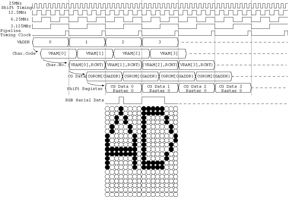
The way of VideoRAM's and Char.ROM's accessing
The image display to the CUI monitor is displaying by the raster-scan like usual TV.
- As for the clock, 75 MHz and 25 MHz are supplied.
The access by the VRAM from the KITE processor synchronizes with 75 MHz.
The CUI control part makes 25 MHz which are the clock of 1dot completely basic and is working.
- As shown in the figure, the side of 1 character becomes 3.125 MHz.
It makes a clock with duty ratio 1/8 a timing clock for the pipeline register at 3.125 MHz to have divided a shift clock (the display clock for 1 dot), 25 MHz in 8 in 25 MHz.
The output-signal
Each output of R, G, the B of the DVI video is 256 pieces of gradation at 8 bits.
However, because the design this time is monochromatic, when making shine, it outputs the case (00) not to make shine R, G, B together (FF).
The sync signal of HS, VS is careful because it is a negative-logic.
DE is asserted (DE=1) when the character display timing.
Note that character display timing is delayed 2-character timing
because of pipelining. So it is careful of not making DEd=1 when the value of HCNT is from 0 to 79.
The sample source
`define HMAX   100 // H total dots
`define HSIZ    80 // H Size
`define HSP     84 // H Sync. Pos.
`define HSL     12 // H Sync. Len.
`define HCR      8 // H dots per Char.
`define VMAX    26 // V total Line
`define VSIZ    24 // V Size
`define VSP     25 // V Sync. Pos.
`define VSL      1 // V Sync. Line
`define VCR     20 // V lines per Char.

module vram ( CLK, DCCLK, RST, ADDR, DATAI, DATAO, MREQ, RW, ACK, R, G, B, HS, VS, DE) ;
   input         CLK,          // Processor Clock (75 MHz)
                 DCLK,         // Video Clock       (25 MHz)
                 RST ;         // Reset
   input  [11:0] ADDR ;        // Video Memory Address
   input  [ 7:0] DATAI ;       // Data Input
   input         MREQ,         // Memory Request
                 RW ;          // Read/Write
   output [ 7:0] DATAO ;       // Data Output
   output        ACK ;         // Acknowledge
   output [ 7:0] R, G, B ;     // RGB Data
   output        HS, VS, DE ;  // Sync. The & Data Enable

   reg     [7:0] DATAO ;

   // Memory
   reg      [7:0] VRAM [0:2047] ;
   reg      [7:0] CGROM [0:4095] ;

   // Counter
   reg      [..:0] CNT ;     // Character Counter (8dots)
   reg      [..:0] HCNT ;    // H Counter 0-99
   reg      [..:0] VCNT ;    // V Counter 0-27
   reg      [..:0] RCNT ;    // R Counter 0-18

   wire          CEP ;     // Character End Pulse

   // Pipeline Register
   reg      [..:0] CADR ;    // Character Code (8bits)
   reg      [..:0] SR ;      // Shift Register (8bits)

   // Internal Signals
   wire     [..:0] VADR ;    // VideoRAM Address (2048bytes)
   wire     [..:0] CGADR ; // CG-ROM Address (4096bytes)
   wire     [..:0] CGDATA;// CG-ROM Data Size (8bits)


  // Memory Initialize
  initial
    begin
      $readmemh ("VRAM20.ram", the VRAM) ;
      $readmemh ("font9x18_256.ram", CGROM) ;
    end

   // Video-RAM Write and Read
   always @ (posedge CLK)
   begin
     if ((ADDR [...] == 1'b1) && MREQ && (RW == ...   ))
         VRAM [... [...:...]]<= ...;
         ... <= VRAM[ ...[...:...]];
   end

   // Video-RAM Acknowledge for Write & Read
   assign ACK = ( ( ADDR[...] == 1'b1 ) && ... );

   // Counter for Character End Pulse
   always @( posedge DCLK )
     if( RST ) ... <= ...     else
               ... <= .......;

   assign ...  = ...;  // Character End Pulse


   always @( posedge DCLK )
   begin
      if( ... ) begin ...<=...; ...<=...; ...<=...; end
      if( ... )
      begin
         if( ... == ... )
         begin
            ... <= ...;
            if( ... == ... )
            begin
               ... <= ...;
               if( ... == ... ) ... <= ...;
               else             ... <= ...;
            end
            else
               ... <= ......;
         end
         else
               ... <= ......;
      end
   end

    // Read character data from VRAM
    always @( posedge DCLK )
    begin
      if( ... )
        begin
          ... <= ...;
        end
    end

   // Internal Memory Address
   assign VADR  = { ..., ... } * 12'd... + { ..., ... };
   assign CGADR = { ..., ...[...:...] };
   assign CGDATA= ...[ ... ];

   // Shift Register
   always @( posedge DCLK )
   begin
      if ( ... ) SR <= ...; else
      if ( ... ) SR <= ...; else
                 SR <= { ..., ... };
   end

   // RGB Data & Data Enable
   assign { R, G, B } = ( ...[...]  && ( RCNT < 16 ) ) ? 24'hffffff : 24'h000000;
   assign DE = ( ( 1 < ... && ... < ... + ... ) && ( ... < ... ) );

   //Sync
   assign HS = ~( HCNT >=   && HCNT (... + ...) ;
   assign VS = ~(VCNT >=... && VCNT < (... + ...)) ;

endmodule
Lastly, it summons as follows from the kite_top hierarchy.
After the clock by PLL is stable about being using LOCKED signal as RST
It is to work a control circuit.
  //
  // Memory and Video RAM
  //
  vram   mem1 ( .CLK(CLK75),
                .DCLK(CLK25),
                .RST(!LOCKED),
                .ADDR(The ADR),
                .DATAI(DATAO[7:0]),
                .DATAO(VRAM_DATAO),
                .MREQ(MREQ),
                .RW(RW),
                .ACK(VRAM_ACK),
                .R(R),
                .G(G),
                .B(B),
                .HS(HS),
                .VS(VS),
                .DE(DE)
              ) ;
| Next |