The simulation method of the VGA module
When not confirming whether or not the counter is working right about the VGA module beforehand by the simulation, easily, as the thinking, it doesn't work.
It creates test bench vram_test for the VGA module.
As for the processor interface, it enters ADDR, DATAI beforehand, as for RW, it enters a suitable value beforehand and it makes MREQ=0 beforehand so as not for Memory Access to occur.
Because nothing goes out of the RGB output when the original value of the VRAM memory is "0", it is initialized beforehand by the suitable character code.
Because the character code writes beforehand in the VRAM20.mem file to copy beforehand by the pre-page, it is possible to use for a test just as it is.
When using Verilog-XL simulator
initial
begin
  $shm_open("waves.shm");
  $shm_probe("as");
end
In writing "WO" beforehand, all of the lower rank hierarchy signal change can be observed with the simulator.
--- vram_test.v ---
`timescale 1 ns of 1ns/
module vram_test ;

reg         CLK, DCLK, RST ;
reg    [11:0] ADDR ;
reg    [7:0] DATAI ;
reg         MREQ
            RW ;
wire [7:0] DATAO ;
wire        ACK ;
wire [7:0] R, G, the B ;
wire        HS, VS, DE ;

initial
begin
  $shm_open("waves.shm") ;
  $shm_probe("as") ;
end

integer i ;

initial
begin
  CLK=0 ;
  for( i=0 ; i<3200000 ; i=i+1 )
     CLK = #10 ~CLK;
  $finish;
end

initial
begin
  DCLK = 0;
  while( 1 )
     DCLK = #20 ~DCLK;
end

initial
begin
  RST = 0;
  RST = #5 1;
  RST = #30 0;
end

initial
begin
  ADDR = 12'h000;
  DATAI= 16'h0000;
  MREQ = 1'b0;
  RW   = 1'b0;
end

vram v1 (CLK, DCLK, RST, ADDR, DATAI, DATAO, MREQ, RW, ACK, R, G, B, HS, VS, DE);

endmodule
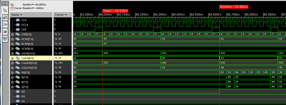
The result of the simulation could be observed as follows.
It is the place where the 2nd lusterware with the 1st line was begun in the cursor location of TimeA.
By the display ending timing CEP for 1 character when counting eight times at 25
MHz of DCLK
0x4B which is the character code to display in CADR which becomes a pipeline
register with this to be output is stored.
Next, it creates CGADR to read the dot data to support 0x4B and it preserves 0x41 which is data in the CGROM memory in shift register SR using the following CEP timing.
In this way, DE which is a display timing signal to be behind in the timing for 2 character and to be output is delayed for 2 characters and the data of the character is output.
When the time progresses, it finds that horizontal synchronization clock HS is output by the negative-logic.
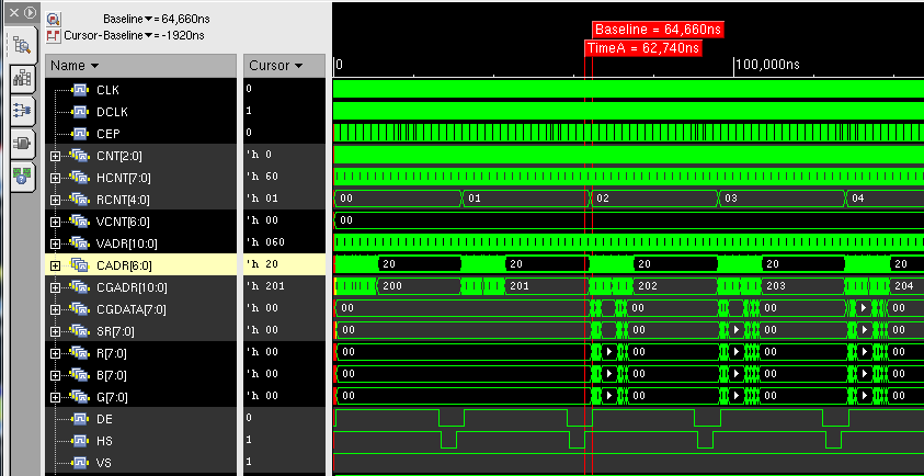
When the time progresses, it finds that vertical-synchronization clock VS is output by the negative-logic.
| Back |