   source /opt/XILINX/Vivado/2015.4/.settings64-Vivado.sh
   vivado &
to execute the design tool.
Push "Create New Project" button for making a new project as "alu".
Push "Next" for first window of "New Project".
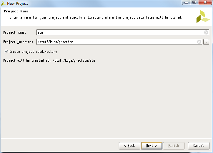
Set "Project name" and "Project location".
And push "Next".
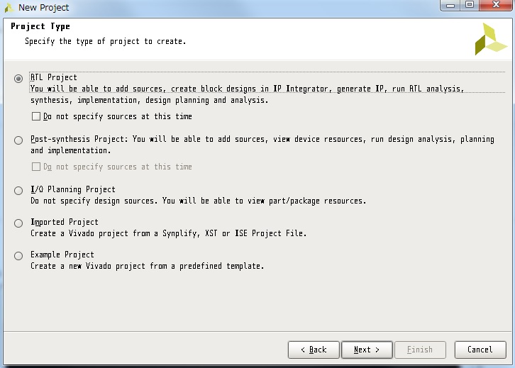
Set "Project Type" to "RTL Project".
And push "Next".
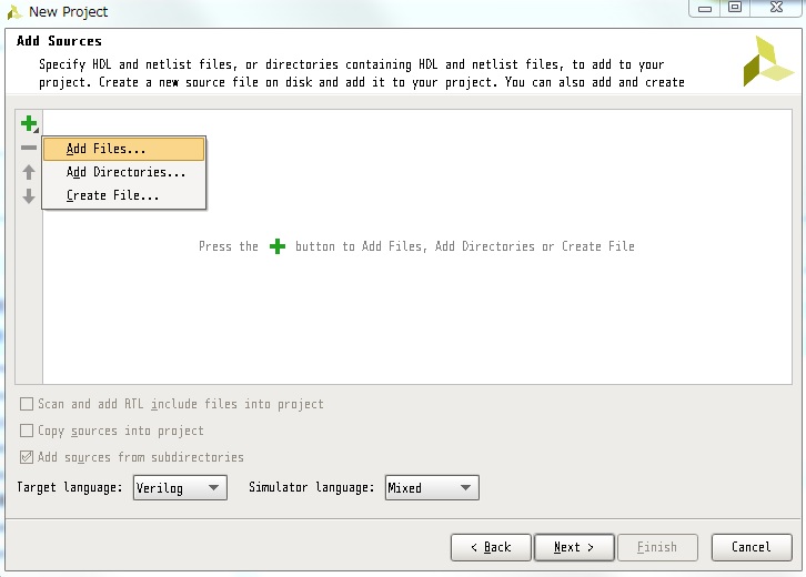
Select "Add Files ..." menu from "+" icon.
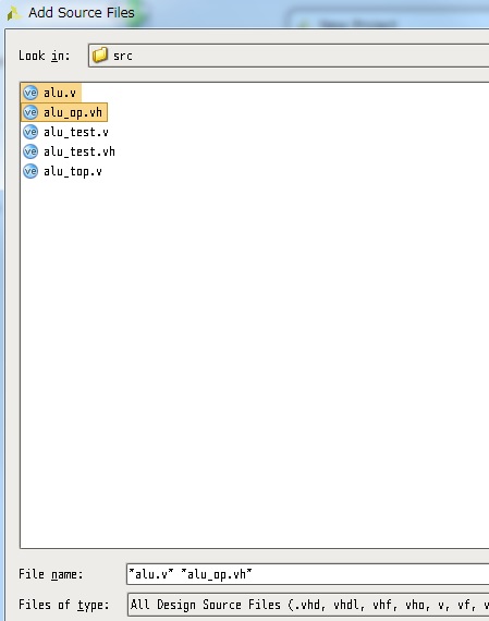
Select "alu.v" and "alu_op.v" files.
And push "OK".
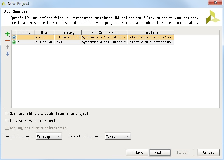
Push "OK" after checking the order of files "alu.v", "alu_op.v".
In next window, "Add Existing IP (optional)", push "Next" for none of setting.
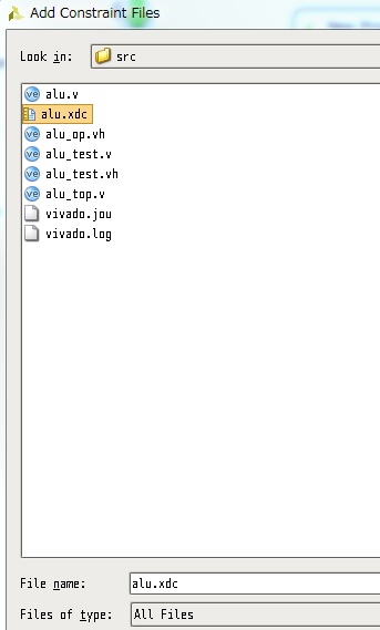
In next "Add Constraints (optional)" window, push "+" icon and push "Add Files...".
THen select "alu.xdc" file for design constraint.
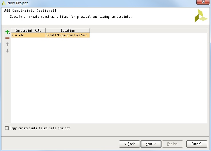
And push "OK" and "Next".
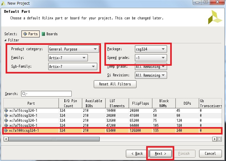
In next "Default Part" window, select a target FPGA device on the NEXYS4 board.
Set following 4 fields for "Filter" setting;
In next window, "New Project Summary", push "Finish".
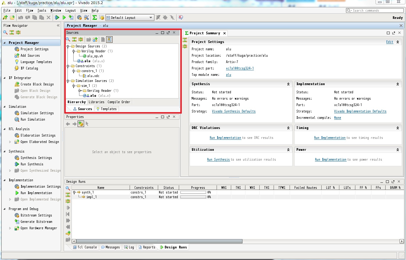
By these steps, the project is generated for ALU implementation shown in following window.
Next, we start implementation process.
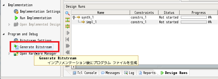
Click "Generate Bitstream" menu from "Flow Navigator" window to start implementation process.
Implementation process includes "Synthesis", "Placing and Routing" and "Bitstream generation".
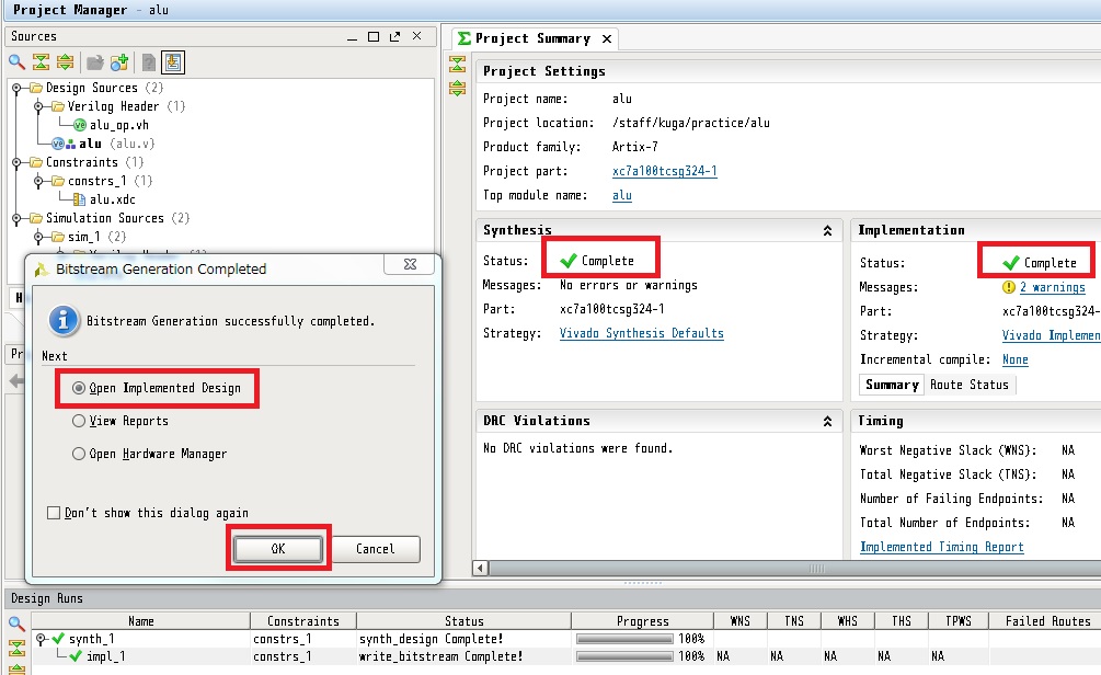
After implementation processes, "Bitstream Generation successfully completed" dialog is appeared.
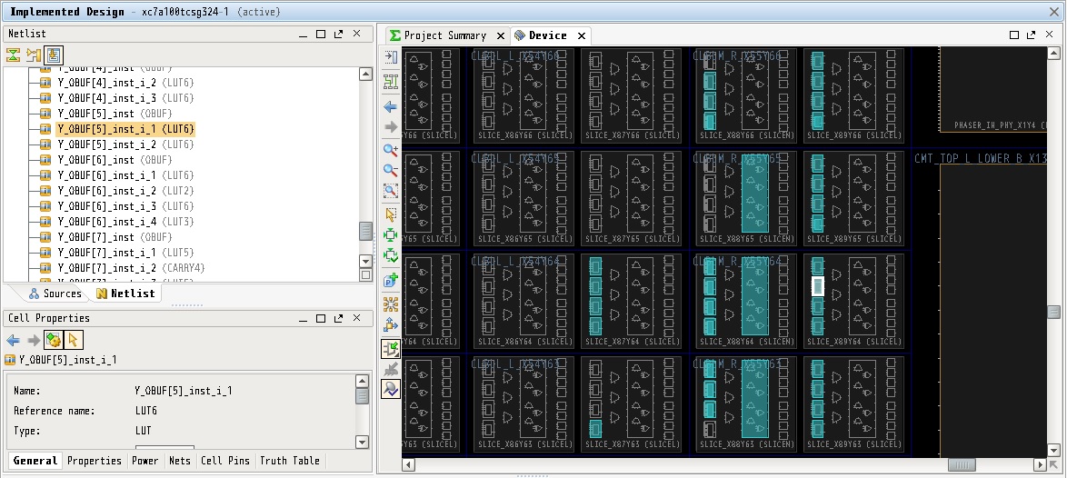
Push "OK", and layout view is displayed in framework window.
Is there no problem in implementation process?
Next, post-layout simulation with real wire delay .