Multiplexer version KITE-1 microprocessor for ATLYS board
Experimentally on KITE, it is using KITE Microprocessor PLUS + board but because the thing with the small implementing scale of FPGA, the interface for the peripheral equipment must be separately developed, this time, it uses the ATLYS board which is made by the DIGILENT Inc. as the implementing board.
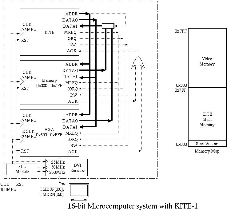
Core processor of the system to try to create is KITE-1 processor and the memory, too, is the simple microprocessor system which contains VGA module with Jules.
It consults the following system block figure and it creates the relation of connection of each module.
The kite_top.v hierarchy to integrate the whole into occurs as follows.
module kite_top(
      CLOCK,      // Clock 100 MHz
      RESET,      // Reset
      TMDSP,      // DVI Video (P)
      TMDSN,      // DVI Video (N)
      ) ;

  input         CLOCK ;
  input         RESET ;
  output [3:0]    TMDSP, TMDSN ;

  //
  // PLL module
  //


  //
  // KITE-1 processor core
  //


  //
  // Memory and Video RAM
  //


  //
  // DVI encoder
  //


endmodule
The arrangement of the PLL module
In the system to design this time, it uses four kinds of clocks.
- The clock for the processor : 75 MHz
- The dot clock for VGA : 25 MHz
- The clock for the DVI encoder : 50 MHz, 250 MHz
Spartan6 to use There is PLL module of the hard macro in FPGA and it can generate 逓倍 and the clock which is necessary in dividing in the clock which was supplied from outside FPGA.
PLL module is described as the instance summon.
Also, it is realized in handing the parameter variable in the PLL module an appropriate value about 逓倍 and the dividing to get a necessary frequency.
Incidentally, LOCKED is the signal which shows that PLL began an operational-stability.
It uses pllfb as the feedback clock by PLL.
  //
  // PLL Module
  //
  wire CLK25, CLK50, CLK75, CLK250, LOCKED, pllfb ;

  pll_module
  #(.C_CLKFBOUT_MULT (15),   // x15
    .C_CLKIN1_PERIOD (10.0), // 100 MHz
    .C_CLKOUT0_DIVIDE (3) ,  // 100*15/2/3=250 MHz
    .C_CLKOUT1_DIVIDE (10) , // 100* February 10th, 15=75 MHz of
    .C_CLKOUT2_DIVIDE (15) , // 100* February 15th, 15=50 MHz of
    .C_CLKOUT3_DIVIDE (30) , // 100* February 30th, 15=25 MHz of
    .C_CLKOUT1_BUF (1)
    .C_CLKOUT2_BUF (1)
    .C_CLKOUT3_BUF (1)
    .C_DIVCLK_DIVIDE (2)     // 2
    )
  pll (
    .CLKIN1 (CLOCK)
    .CLKOUT0 (CLK250)
    .CLKOUT1 (CLK75)
    .CLKOUT2 (CLK50)
    .CLKOUT3 (CLK25)
    .RST (RESET), .LOCKED (LOCKED), .CLKFBIN (pllfb), .CLKFBOUT (pllfb)
    ) ;
It copies source of PLL module from this place. Pass beforehand.
Incidentally, it is provided in the VHDL hardware description language.
When using KITE-1 processor as the IP core, it doesn't use most signal for the observation which goes out of KITE-1.
The input/output signal of the kite.v hierarchy uses only the following signal.
※ Unused wire is deleted by the optimization
process in implementing..
  //
  // KITE-1 processor core
  //
  kite kite( .DATAI(DATAI),       // in  DATA Bus
             .DATAO(DATAO),       // out DATA Bus
             .ADDR(ADR),          // Address Bus
             .HALT(HALT),         // HALT Signal
             .MREQ(MREQ),         // Memory Request
             .IORQ(IORQ),         // I/O Request
             .ACK(ACK),           // Acknowledge
             .RW(RW),             // Read/Write
             .CLK(CLK75),         // Clock
             .RST(RST),           // Reset
             .ICS(ICS)            // Instruction Complete Signal
        );
It is therefore explained next-page since then to the details of the memory module, the UCI module, the DVI encoder module.
Next, it creates a memory module.
| Back
|