The video module and the DVI encoder module cling.


It adds to the built-in system which creates a created video module.
After choosing the video module which was subscribed into "IP Catalog" of the XPS window in computer graphics like the following figure by the left click of the Mus, click the right of the Mus and let it display a menu and it chooses "Add IP" on the left of the Mus.


" The small window in computer graphics, Add IP Instance to Design", rises up but this presses OK.
Next, following "XPS Core Config" window in computer graphics rises up.


The allocating place of the memory which is used when installing a video module must make the Ort which is the same as the memory which is already installed in the processor not become.

To 0x45000000 of "C_MEM0_BASEADDR"
To 0x4500ffff of "C_MEM0_HIGHADDR"
It changes "C_S_AXI_MIN_SIZE" into 0x0000ffff and it presses OK.

" The Instantiate and Connect IP" window in computer graphics rises up.
To connect a video controller with "microblaze_0", it presses OK just as it is.
A video module is added to the place of "Bus Interfaces" as "vga_0" by this.
Also, when clicking + which is in front of "vga_0" of "Bus Interfaces", like the following figure, "S_AXI" which is can be confirmed in "PUROSESSABASU" of the video module and it is possible to confirm that it is connected with "axi4lite_0" which is in "Processor Local Bus".


It installs a DVI encoder module.

In the same way, it adds a DVI encoder module.
" After choosing the DVI encoder module IP which was subscribed into IP Catalog" by the left click of the Mus, click the right of the Mus and let it display a menu and it chooses "Add IP" on the left of the Mus.


" The small window in computer graphics, Add IP Instance to Design", rises up but this presses OK.
Next, it presses OK just as it is because the "XPS Core Config" window in computer graphics rises up but there is not ݒ"RU" entry specifically this time. Like the following figure, a DVI encoder module is added as "dvi_out_native".


Next, it clicks + which is in front of "dvi_out_native_0" of "Bus Interfaces".
The office of productivity, technology and innovation of "Bus Name" becomes "No Connection" like the figure above and the distribution of "DVI_VIDEO_IN" isn't yet connected with the "vga" module right.

Like the following figure, it makes "No Connection" become "vga_0_DVI_VIDEO_OUT".
"DVI_VIDEO_OUT" of the "vga" module is connected with "DVI_VIDEO_IN" of the DVI encoder module by this.


Next, it does the establishment of the input-output pin about the "Ports" tab.
" It clicks + which is in front of External Ports" and "dvi_out_native_0".
The output terminal of TMDS, TMDSB which becomes an output from "dvi_out_native_0" to the LCD monitor is displayed, but nothing is displayed in the office of productivity, technology and innovation of "Connected Port" and nothing is connected.


It presses the right of the Mus in the office of productivity, technology and innovation of "Connected Port" of "dvi_out_native_0" like the following figure.
" It chooses Make External".


It is changed with the distribution first name which a chosen chromosome-segment was automatically put to and the output terminal of "dvi_out_native_0_ signal name " is added to the office of productivity, technology and innovation of "External Ports", too.


The distributions such as the clock

In the system this time, it uses three of 75 MHz, 150 MHz, 750 MHz as the clock.
Being as the initial installation prepares two clocks later only for a 75-MHz clock to be prepared.
It is "Configure IP. in the place of "clock_generator_0". It starts up ".


The "XPS Core Config" window in computer graphics like the following figure rises up.


As for the configuration of "CLKOUT1" and "CLKOUT2", "Required Frequency" of "CLKOUT1" becomes as follows the catastasis which can not be chosen about 0 Hz, "CLKOUT2".


It makes "Required Frequency" of "CLKOUT1" 750000000 Hz (750 MHz) as follows and also in this, it makes "Buffered" of "CLKOUT1" FALSE.
Next, because "CLKOUT2" becomes able to be entered, it makes "Required Frequency" 150000000 Hz (150 MHz).
Incidentally, there is "Buffered" of "CLKOUT2" as "TRUE".
It presses OK above.


The configuration of the clock-generation module was made of this but the distribution of the clock isn't yet connected.
It sets "clkx10in" of "dvi_out_native_0" to "clock_generator_0::CLKOUT1" like the following figure.
In in the same way "clock_generator_0::CLKOUT2" of "clkx2in" of "dvi_out_native_0"
It sets "clkin" of "dvi_out_native_0" to "clock_generator_0::CLKOUT0".


Also, "pll_lckd" which is "reset" which is a reset signal and the input signal to know that the clock is working normally, too, is left in the non-distribution in "dvi_out_native_0".
In "proc_sys_reset_0::MB_Reset" that "reset" is the output-signal of the reset module like the figure above
"pll_lckd" wires "clock_genetator_0::LOCKED" which is the output-signal of the clock module.

The acknowledgement of the address space

Next, it chooses "Addresses" tab.
It confirms that a video module is allocated for the memory space of the 64k 8-bit byte to address 0x45000000-0x4500FFFF.
Also, it confirms that pushdown-switch "Push_buttons_5Bits" is allocated for the memory space of the 64k 8-bit byte to address 0x40000000-0x4000FFFF.
When different, it changes as it becomes 0x40000000-0x4000FFFF.
The address at the head of this address becomes a necessary later when creating a program.


The configuration of the FPGA output terminal The output terminals TMDS and TMDSB of "dvi_out_native_0" must be made to be able to connect with the extraction LCD monitor as the output from FPGA.
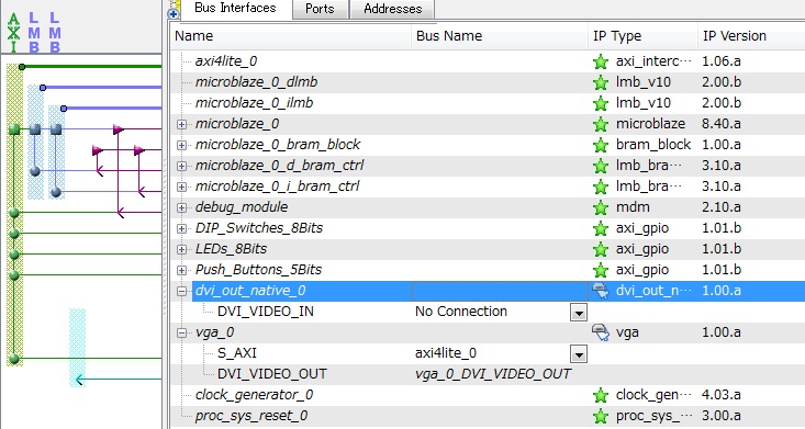
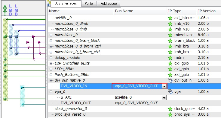
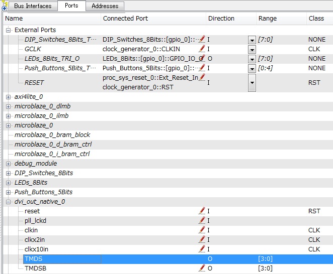
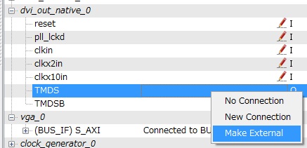
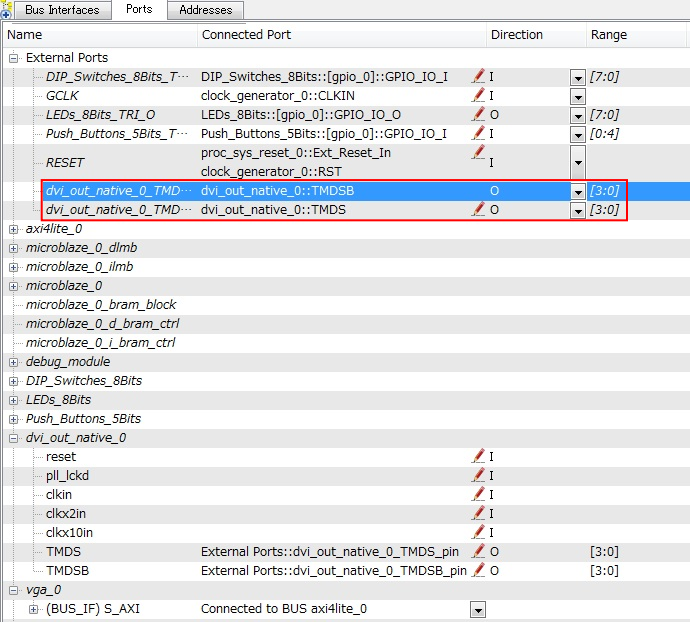
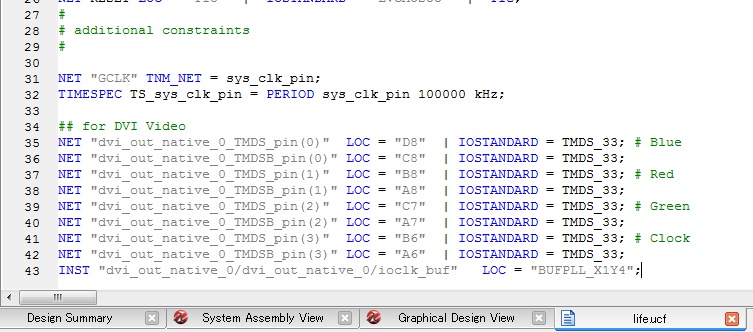
The configuration to allocate output terminals TMDS and TMDSB in the physical electric terminal of FPGA is described.

"UCF File of choosing "Project" tab : It clicks the office of productivity, technology and innovation of data/life.ucf" in the double.
The edit-display of the "life.ucf" file starts up.


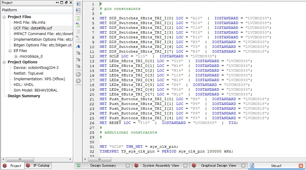
It adds the following account to the office of productivity, technology and innovation of the last-line of the file.
## for DVI Video
NET "dvi_out_native_0_TMDS_pin(0)"  LOC = "D8"  | IOSTANDARD = TMDS_33; # Blue
NET "dvi_out_native_0_TMDSB_pin(0)" LOC = "C8"  | IOSTANDARD = TMDS_33;
NET "dvi_out_native_0_TMDS_pin(1)"  LOC = "B8"  | IOSTANDARD = TMDS_33; # Red
NET "dvi_out_native_0_TMDSB_pin(1)" LOC = "A8"  | IOSTANDARD = TMDS_33;
NET "dvi_out_native_0_TMDS_pin(2)"  LOC = "C7"  | IOSTANDARD = TMDS_33; # Green
NET "dvi_out_native_0_TMDSB_pin(2)" LOC = "A7"  | IOSTANDARD = TMDS_33;
NET "dvi_out_native_0_TMDS_pin(3)"  LOC = "B6"  | IOSTANDARD = TMDS_33; # Clock
NET "dvi_out_native_0_TMDSB_pin(3)" LOC = "A6"  | IOSTANDARD = TMDS_33;
INST "dvi_out_native_0/dvi_out_native_0/ioclk_buf"   LOC = "BUFPLL_X1Y4";
After adding, it is as follows.
Press to save the file.


Above, it is finished the hardware design of the system.
Next, it is layout process for embedded system.
| Back |Top |Next |